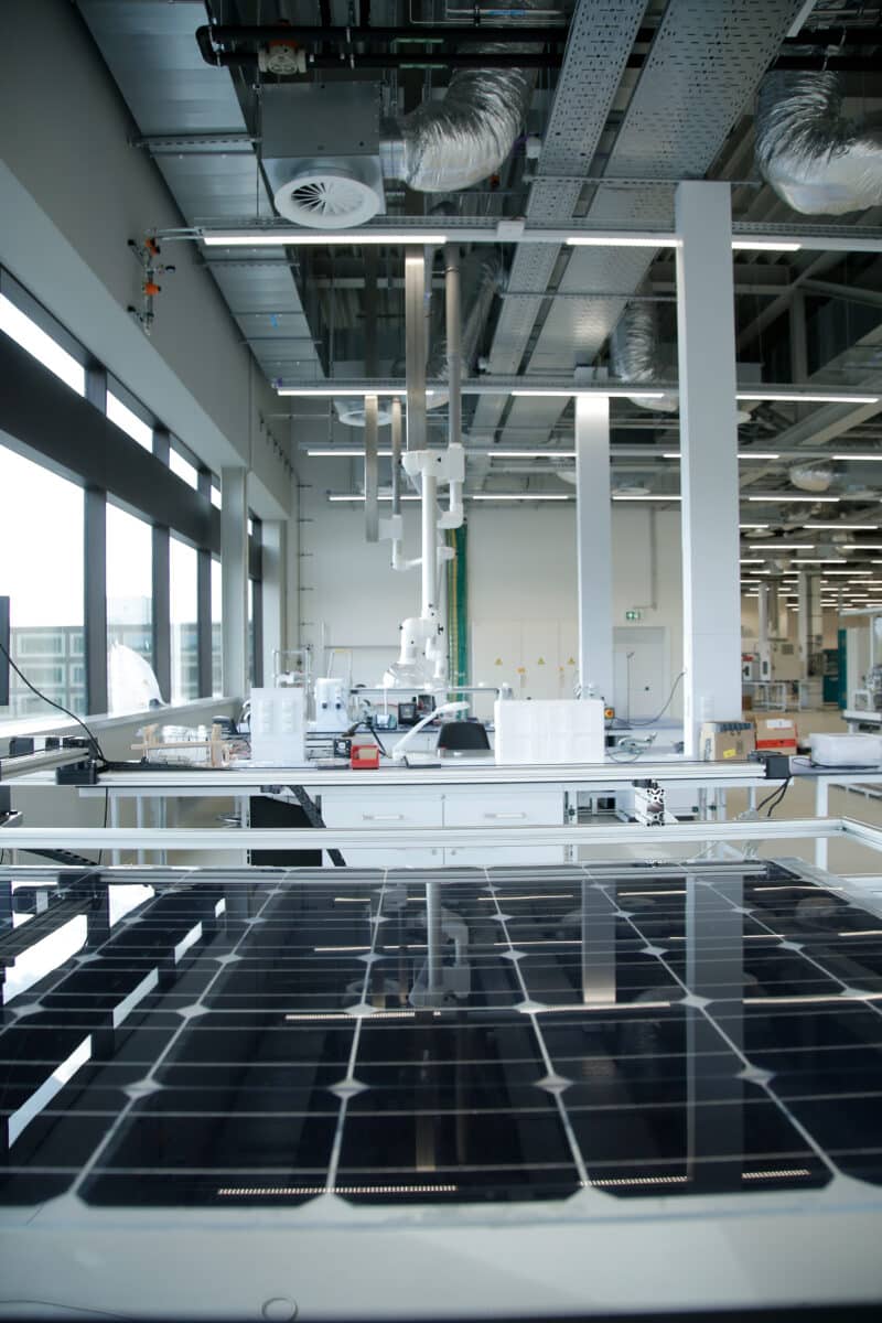
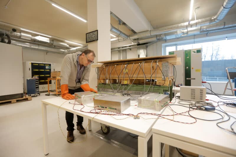
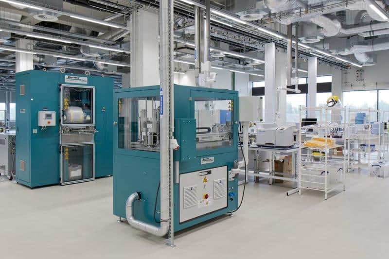
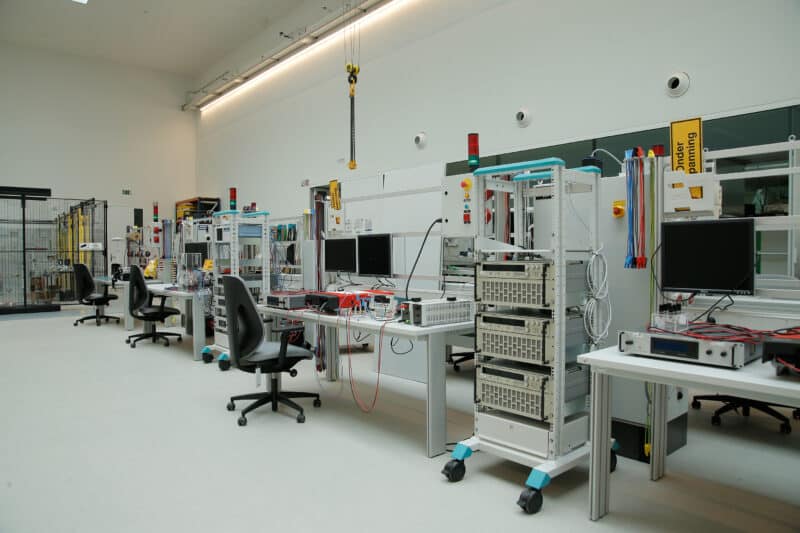
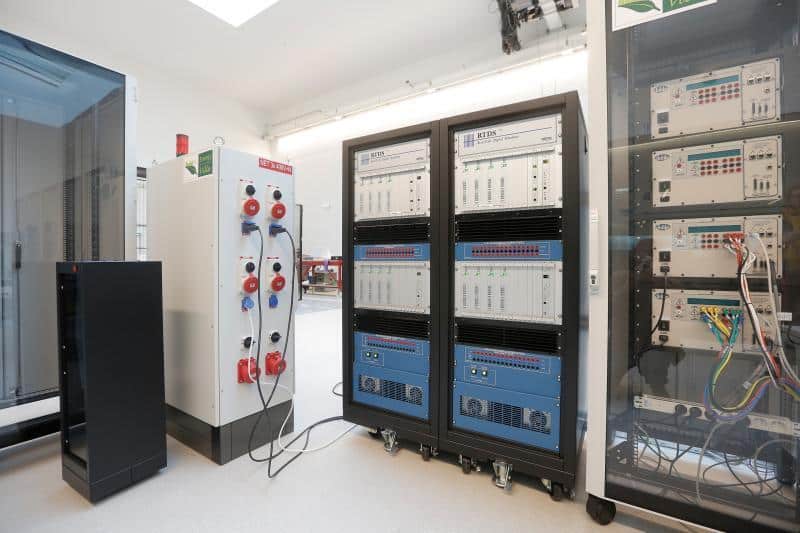
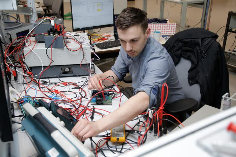
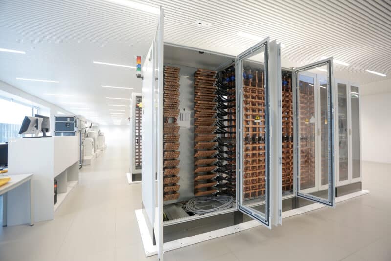
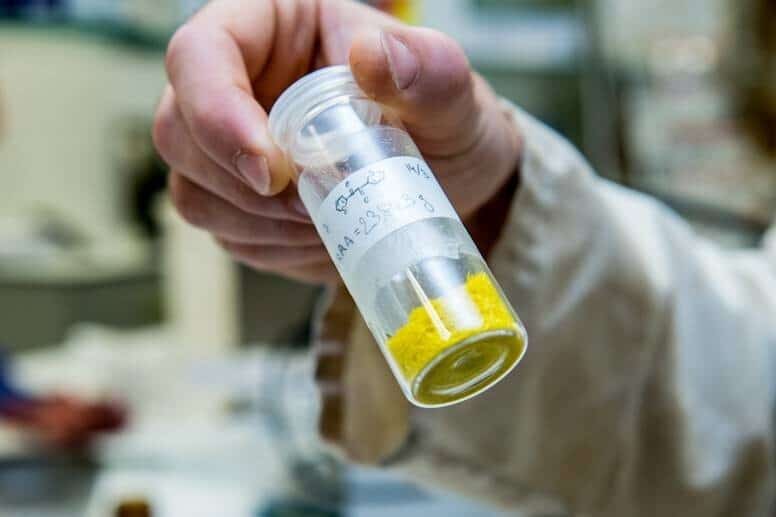
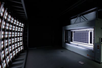
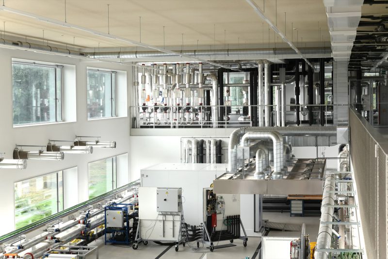
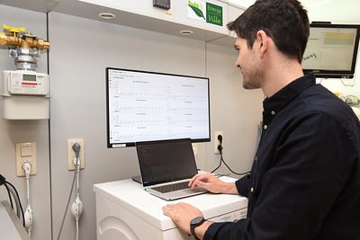
Fabrication and characterisation of PV moduleLaminators

The PV Module Lab infrastructure is designed for fabrication and characterisation of PV modules with equipment that is state-of-the-art and/or beyond. As such, it is well-suited to evaluate and process both standard and new materials in the PV module value chain: cells, interconnect structures, encapsulants, backsheets and glass. Additionally, the versatility of the equipment allows for standard flat commodity PV as well as early-stage development of new interconnection and encapsulation technologies in an exploratory phase, while the same tools simultaneously accommodate scaling up to full-size panels (1m x 1.6m).

Bart Onsia

Contact

Bart Onsia

Business Developer Solar, Batteries and Power to Molecules at EnergyVille/imec
Description
Technical Notes

AdvantagesEV2 solar lab

Additional to the availability of advanced tools , the infrastructure is operated by experienced engineers and researchers for the development of next-generation PV module and interconnection technologies. The team members have an extensive background in PV materials, concept definition and proof, industrial (best) practices for standard and BIPV fabrication, characterisation and reliability, as well as in-depth knowledge of detailed solar cell (optical, electrical and thermal) behaviour and how this behaviour is translated into modules and systems (both in theory and in a practical implementation). In this way, we can carry out new technology development and offer objective technology advice taking into account the overall perspective as well as the slightest details.

Applications

Processing designed for the fabrication of wafer-based crystalline-Si PV modules (or similarly applied in thin-film or an even
broader technology context):

  • Laser processing
  • Placement
  • Dispensing
  • Soldering
  • Lamination

In-depth testing of the optoelectronic performance of devices (fabricated in our labs or elsewhere):

  • Optical inspection
  • Light IV
  • Dynamic illumination
  • Electroluminescence (EL)
  • External quantum efficiency (EQE)
  • Reflection (R)
  • (Cross-section) scanning electron microscopy (SEM)
  • SunsVoc (dependency of Voc on irradiance intensity)
  • Thermal and spectral dependencies in behaviour
  • Pull testing

Most of the equipment offers the opportunity of automation for its designated processing/testing, though the loading and unloading (and in some cases mechanical movement) are done manually to ensure the highest versatility in operation. Manual
preparations, rework and inspection can be done offline with state-of-the-art lab tables and tools. Dry room storage (0.4%RH) is available for moisture sensitive materials (e.g. encapsulants).

Customers

  • PV cell and module manufacturers
  • Material suppliers
  • Equipment vendors
  • PV system builders and operators
  • (*)Laser processing: high-resolution (scanhead) laser at 1070 nm and 15kW peak power, designed for cutting of metal
  • wires and scribing of silicon cells
  • (*)Placement: high-resolution (±0.2 mm) gantry for automated layup (pick and placement) of silicon cells and (interconnect) foils with Bernouilli and vacuum gripping
  • Dispensing
    • (*)High-resolution (±0.2 mm) dispensing with Auger valve for highly accurate (0.001g) volumes designed for solder pastes
    • State-of-the-art dispensing based on pulsed dosing with compressed air designed for solder pastes and sealants
  • Soldering with high-temperature accuracy and flexible programming of soldering profiles (up to 400°C)
    • (*)Beyond state-of-the art hot-air soldering with programmable air flow and temperature
    • State-of-the-art industrial tabbing-stringing-based contact soldering
  • Lamination with flexible programming of lamination profiles
    • Beyond state-of-the-art high-accuracy flat-plate lamination allowing standard as well as inverse lamination cycles for highly accurate temperature-time-pressure profiles (up to 180°C). Lamination on lightly curved surfaces is possible.
    • Small-area lamination for quick testing (up to 250°C) up to 60x 60 cm2
  • Optical inspection
    • Large-area (1x1.6m²) high-resolution (<0.2 mm) inspection with optional automation and stitching
    • Small-area microscopy for optical (and SEM) inspection of detailed areas or cross-sections
  • Light IV for accurate IV-sweeping of devices (up to 15A and 200V)
    • Large-area illumination with LED-based spectrum- and intensity-tunable light source (18 colours 0.1-1.2 suns), temperature control (10-80°C) and optional 2-side illumination (for bifacial modules), designed for large PV modules (up to 1.6m²)
    • Small-area tool designed for detailed inspection of cells and mini-modules
  • Dynamic illumination with angular control and intensity-tunable and time-programmable LED tubes
  • Electroluminescence (EL) for high-quality defect imaging
    • High-resolution automated inspection in fixed setup
    • Mobile setup for “fast and anywhere” testing
  • External quantum efficiency (EQE) scanning for accurately determining spectral electrical sensitivity of devices in 300-1200 nm range
  • Reflection (R) scanning for accurately determining spectral reflective sensitivity of devices in 300-1200 nm range
  • Pull testing of materials with highly accurate control and monitoring of location, speed, load and strain designed for determination of mechanical yield stress, adhesion strength and shear forces through peeling (possible at different angles) relevant for PV modules (e.g. encapsulant adhesion, solder joint strength...)

(*) in acquisition phase