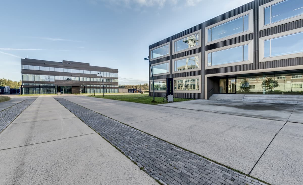
Research
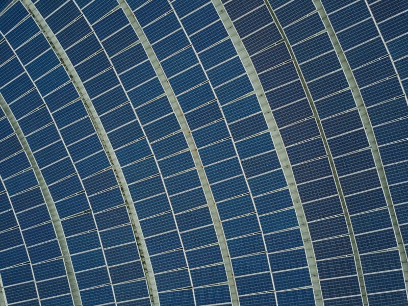
Groundbreaking renewable energy research
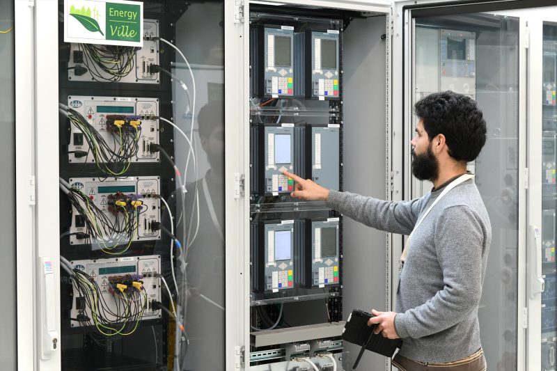
With a comprehensive approach covering every aspect of the energy system, we combine the expertise of our four renowned partners – KU Leuven, VITO, imec and UHasselt. What makes EnergyVille unique is the exceptional synergy between our research partners, allowing us to seamlessly integrate every aspect of the energy system value chain. From materials and components to complete energy systems, business models and strategic initiatives; excellent research across the entire value chain is what we stand for.
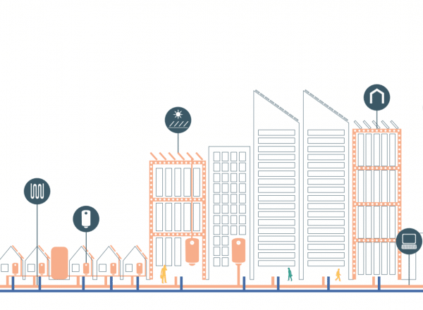
Our efforts are organized into eight interdisciplinary areas, each representing a critical piece of the puzzle. Explore the various themes in which we excel and discover the potential of a more sustainable, efficient energy system for the future.