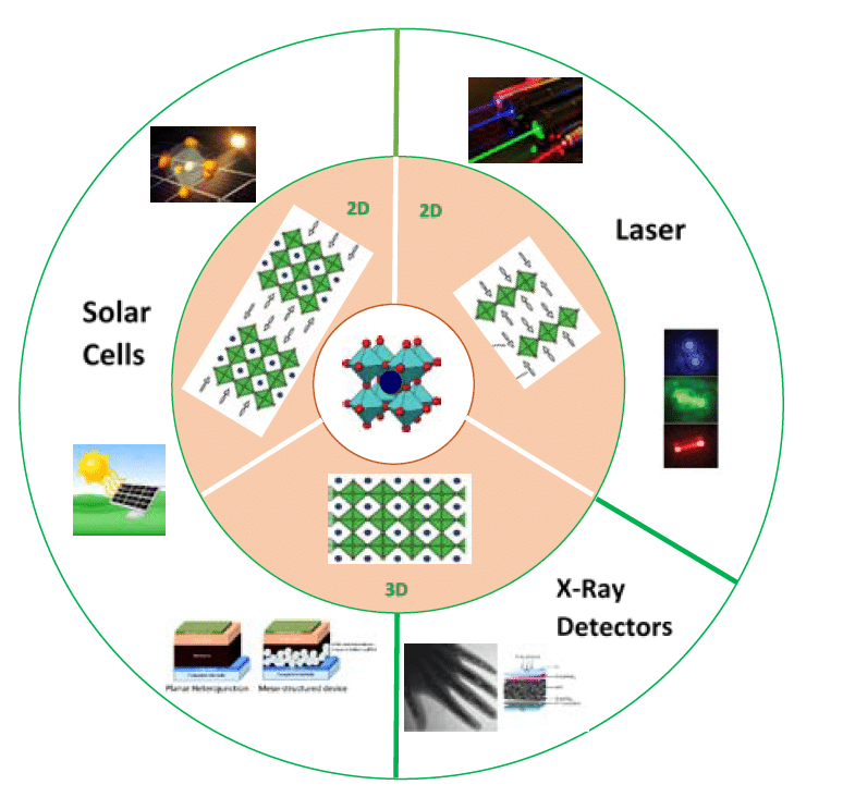
PROCEED: perovskites move beyond solar cells and revolutionise laser-based projectors and X-ray imaging
Perovskites are mainly known in the field of solar cells. Researchers from IMO-IMOMEC, within EnergyVille, and colleagues from KU Leuven, UGent and UAntwerpen, are tuning perovskites also for other applications. It is the combination of good opto-electronic properties with low material and manufacturing costs that makes perovskites a promising material for any application in which light absorption, emission and detection is involved.
Together with several leading companies (i.e. Agfa NV and ENGIE Laborelec), the team will explore what perovskites can do for X-ray and lasers, as well as for solar cells. For X-ray detectors, the use of perovskites could lead to improved image quality, which can be translated into significantly lower exposure levels for medical or security screening of humans. For lasers, the new material development aims at increasing the material gain coefficient to 1000cm-1 or more, resulting in more cost-effective projectors with better resolution. For solar cells, perovskite materials with enhanced moisture and thermal stability will be developed.
The holy grail of perovskites
Perovskite is a family of materials that has been known for some time because of its intriguing physical properties. It has been studied e.g. as a piezoelectric material, as superconductor, or to catalyse chemical processes.
Laurence Lutsen (EnergyVille/UHasselt): “A key characteristic of hybrid perovskites is its astonishing versatility, both in terms of composition, dimension and morphology. First of all, the composition of metal halide perovskites can vary: if you take the generic chemical formula ‘APbX3’, X can either be chlorine, bromine or iodine, whereas A stands for different possible cations such as methylammonium, formamidimium or cesium. Second, thanks to this compositional freedom, material scientists can create hybrid perovskites with different dimensionality, going from regular 3D[1] materials to materials that have an intrinsic (quasi-)2D or even 0D structure. And thirdly, perovskites can be synthesized with many different morphologies, such as thin films, single crystals, microcrystals or nanocrystals.”
Perovskites for solar cells: towards 2D perovskites for more stability
Crystalline silicon-based technologies are currently dominating the PV market. Typical commercial module efficiencies are about 17-18%, with a record commercial product efficiency of 22.8% and the theoretical limit being over 29%. One way to reach a higher conversion efficiency, is by stacking different semiconductor materials, each with their specific bandgap. Each layer is suited for a specific part of the light spectrum and in this way higher efficiencies can be reached.
Tandem solar cells combining silicon and perovskite solar cells could be the answer to solar cells exhibiting both high efficiency and low costs. The low cost of a perovskite-based solar cell comes from the fact that the material itself is not expensive, only thin films are used and the process technology via printing/coating is relatively simple and doesn’t require any expensive equipment.
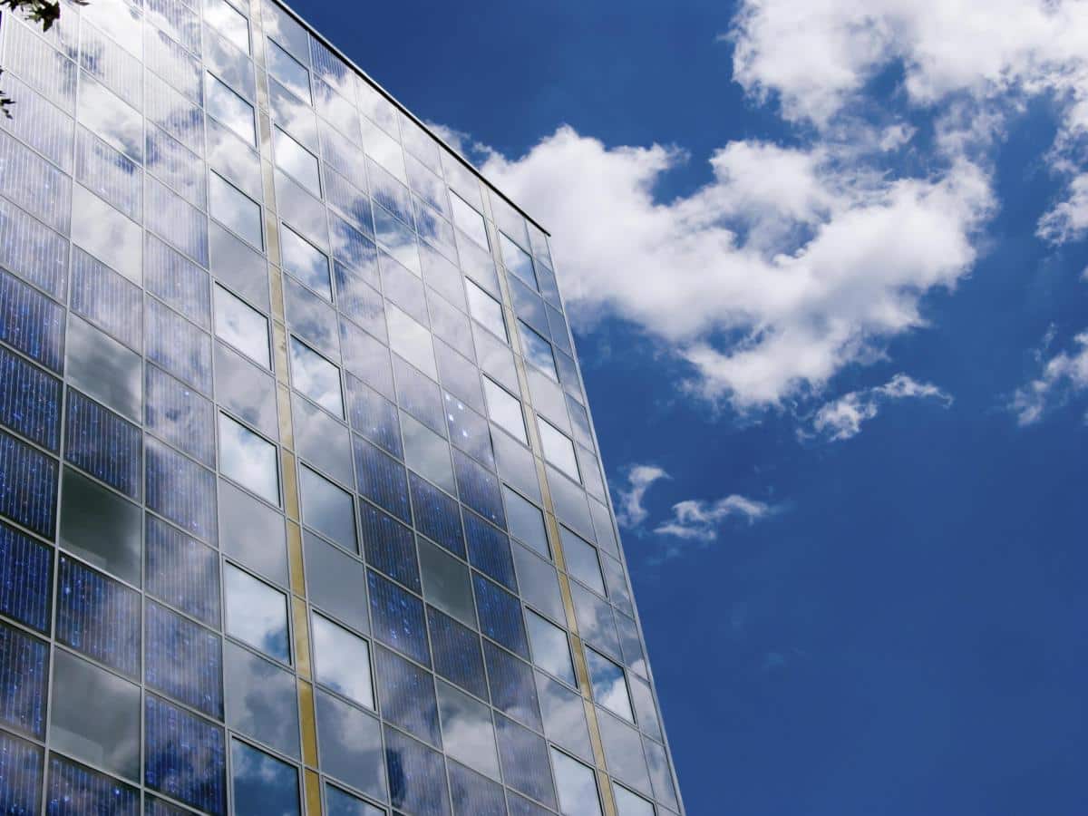
Moreover, because of their semi-transparency, their light weight and the possibility to produce them on flexible substrates, they are ideal candidates for BIPV (Building Integrated Photovoltaics). The ease of processing allows for customization in dimensions as well as in design (color, transparency), an important asset to convince architects of using more solar technology into their buildings. And, because the efficiency decreases less at higher temperatures (as compared to crystalline silicon solar cells) they could be integrated in insulating glazing. Next to that, perovskite solar cells could be integrated into roof, architectural glass, walls, tiles, facades and shingles. In these cases, the orientation of the solar cells is less of an issue because of the better response to diffuse light conditions than silicon solar cells.
Perovskite as a material platform for other applications
Because perovskites are so versatile, they could be used for other applications too. Until now, mainly solar cells were on the agenda of perovskite material developers and researchers. And although there are still some major issues with perovskite-based solar cells, it is worthwhile to explore and tune perovskite chemical structures also for other applications. Laurence Lutsen: “In Proceed, the consortium is developing novel 3D/2D perovskite structures to tackle the stability issue in solar cells but also focusing on fabricating thick perovskite films with large dimensions for X-ray applications, and perovskite nanocrystals as gain material for lasers for light projectors. In all these cases, the use of perovskites promises a lower cost and better performance.”
Perovskites for X-ray: thick and large layers are key
In recent years, perovskite materials based on high Z elements have been tested for X-ray detection in order to make high image quality detectors for general radiography applications, allowing reduced radiation dosage for patients. As perovskite layers can be applied by low cost methods at low temperature even on flexible substrates, this new approach would make a low cost, low weight, robust, large format and potentially flexible X-ray detector feasible. This would enable the broader use of X-ray scanners for health applications (human and veterinary), for industrial use and for security. Industrial detectors can e.g. be used for non-destructive quality control in industrial branches such as automotive, aerospace, defense and power generation. Also, in security domains, X-ray is a growing market because of the globalized traffic and trade and the growing need to scan people and cargos at the border checkpoints.
Perovskites for light projectors: nanocrystals to ‘pump up’ the lasers
Light sources for light projectors need to reproduce as many visible colors as possible, with high brightness and minimal power consumption. Lasers are ideal candidates for this and have a much better performance and lifetime as compared to the traditional high-pressure lamps (in the case of projectors).
Current laser projection systems use a focused blue laser to pump a luminescent material such as YAG:Ce to generate the red, green and blue primary colors from a point source. This approach has a limited optical efficiency. Laurence Lutsen: “It would be possible to combine a commercial blue laser – the most performing of the red/green/blue set – with low-cost, optically pumped red and green amplified spontaneous emission sources or lasers. Perovskite nanocrystals could be used as green or red gain material and this approach would reduce the complexity and cost (a large cost reduction of 30-40% for the projector light source is expected) of high-end laser projectors. The tunable bandgap and high optical gain of perovskites are important in this context.”